- 您现在的位置:买卖IC网 > Sheet目录3876 > PIC18F4580T-I/ML (Microchip Technology)IC PIC MCU FLASH 16KX16 44QFN
2010 Microchip Technology Inc.
DS21801F-page 43
MCP2515
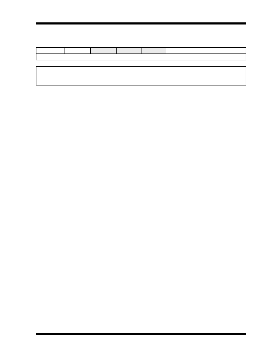
REGISTER 5-3:
CNF3 - CONFIGURATION 1 (ADDRESS: 28h)
R/W-0
U-0
R/W-0
SOF
WAKFIL
—
PHSEG22
PHSEG21
PHSEG20
bit 7
bit 0
Legend:
R = Readable bit
W = Writable bit
U = Unimplemented bit, read as ‘0’
-n = Value at POR
‘1’ = Bit is set
‘0’ = Bit is cleared
x = Bit is unknown
bit 7
SOF: Start-of-Frame signal bit
If CANCTRL.CLKEN = 1:
1
= CLKOUT pin enabled for SOF signal
0
= CLKOUT pin enabled for clockout function
If CANCTRL.CLKEN = 0, Bit is don’t care.
bit 6
WAKFIL: Wake-up Filter bit
1
= Wake-up filter enabled
0
= Wake-up filter disabled
bit 5-3
Unimplemented: Reads as ‘0’
bit 2-0
PHSEG2: PS2 Length bits<2:0>
(PHSEG2 + 1) x TQ
Minimum valid setting for PS2 is 2 TQ
发布紧急采购,3分钟左右您将得到回复。
相关PDF资料
PIC18F25K20-I/ML
IC PIC MCU FLASH 16KX16 28QFN
PIC16F724-I/P
IC PIC MCU FLASH 4KX14 40-DIP
PIC18LF8310T-I/PT
IC PIC MCU FLASH 4KX16 80TQFP
PIC18LF8390T-I/PT
IC PIC MCU FLASH 4KX16 80TQFP
PIC24F16KL401-I/MQ
IC MCU 16BIT 16KB FLASH 20-QFN
PIC18F2431T-E/SOG
IC PIC MCU FLASH 8KX16 28SOIC
DSPIC30F6015-20I/PT
IC DSPIC MCU/DSP 144K 64TQFP
DSPIC30F6014A-20I/PT
IC DSPIC MCU/DSP 144K 80TQFP
相关代理商/技术参数
PIC18F4580T-I/PT
功能描述:8位微控制器 -MCU 32 KB FL 1536 RAM 36 I/O RoHS:否 制造商:Silicon Labs 核心:8051 处理器系列:C8051F39x 数据总线宽度:8 bit 最大时钟频率:50 MHz 程序存储器大小:16 KB 数据 RAM 大小:1 KB 片上 ADC:Yes 工作电源电压:1.8 V to 3.6 V 工作温度范围:- 40 C to + 105 C 封装 / 箱体:QFN-20 安装风格:SMD/SMT
PIC18F4585-E/ML
功能描述:8位微控制器 -MCU 48KB 3328 RAM w/ECAN RoHS:否 制造商:Silicon Labs 核心:8051 处理器系列:C8051F39x 数据总线宽度:8 bit 最大时钟频率:50 MHz 程序存储器大小:16 KB 数据 RAM 大小:1 KB 片上 ADC:Yes 工作电源电压:1.8 V to 3.6 V 工作温度范围:- 40 C to + 105 C 封装 / 箱体:QFN-20 安装风格:SMD/SMT
PIC18F4585-E/P
功能描述:8位微控制器 -MCU 48KB 3328 RAM w/ECAN RoHS:否 制造商:Silicon Labs 核心:8051 处理器系列:C8051F39x 数据总线宽度:8 bit 最大时钟频率:50 MHz 程序存储器大小:16 KB 数据 RAM 大小:1 KB 片上 ADC:Yes 工作电源电压:1.8 V to 3.6 V 工作温度范围:- 40 C to + 105 C 封装 / 箱体:QFN-20 安装风格:SMD/SMT
PIC18F4585-E/PT
功能描述:8位微控制器 -MCU 48KB 3328 RAM w/ECAN RoHS:否 制造商:Silicon Labs 核心:8051 处理器系列:C8051F39x 数据总线宽度:8 bit 最大时钟频率:50 MHz 程序存储器大小:16 KB 数据 RAM 大小:1 KB 片上 ADC:Yes 工作电源电压:1.8 V to 3.6 V 工作温度范围:- 40 C to + 105 C 封装 / 箱体:QFN-20 安装风格:SMD/SMT
PIC18F4585-H/ML
功能描述:8位微控制器 -MCU 48 KB Flash 3328 RAM 36 I/O w/ECAN RoHS:否 制造商:Silicon Labs 核心:8051 处理器系列:C8051F39x 数据总线宽度:8 bit 最大时钟频率:50 MHz 程序存储器大小:16 KB 数据 RAM 大小:1 KB 片上 ADC:Yes 工作电源电压:1.8 V to 3.6 V 工作温度范围:- 40 C to + 105 C 封装 / 箱体:QFN-20 安装风格:SMD/SMT
PIC18F4585-H/P
功能描述:8位微控制器 -MCU 48 KB Flash 3328 RAM 36 I/O w/ECAN RoHS:否 制造商:Silicon Labs 核心:8051 处理器系列:C8051F39x 数据总线宽度:8 bit 最大时钟频率:50 MHz 程序存储器大小:16 KB 数据 RAM 大小:1 KB 片上 ADC:Yes 工作电源电压:1.8 V to 3.6 V 工作温度范围:- 40 C to + 105 C 封装 / 箱体:QFN-20 安装风格:SMD/SMT
PIC18F4585-H/PT
功能描述:8位微控制器 -MCU 48 KB Flash 3328 RAM 36 I/O w/ECAN RoHS:否 制造商:Silicon Labs 核心:8051 处理器系列:C8051F39x 数据总线宽度:8 bit 最大时钟频率:50 MHz 程序存储器大小:16 KB 数据 RAM 大小:1 KB 片上 ADC:Yes 工作电源电压:1.8 V to 3.6 V 工作温度范围:- 40 C to + 105 C 封装 / 箱体:QFN-20 安装风格:SMD/SMT
PIC18F4585-I/ML
功能描述:8位微控制器 -MCU 48KB 3328 RAM w/ECAN RoHS:否 制造商:Silicon Labs 核心:8051 处理器系列:C8051F39x 数据总线宽度:8 bit 最大时钟频率:50 MHz 程序存储器大小:16 KB 数据 RAM 大小:1 KB 片上 ADC:Yes 工作电源电压:1.8 V to 3.6 V 工作温度范围:- 40 C to + 105 C 封装 / 箱体:QFN-20 安装风格:SMD/SMT